TSMC’s Super-gap Approach Puts Samsung Electronics on Alert

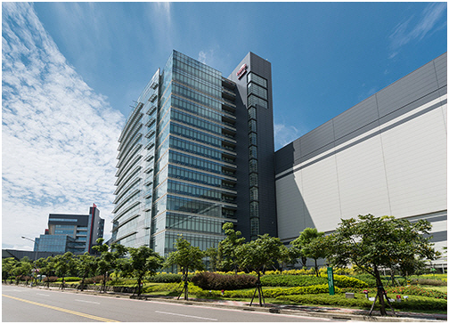
TSMC’s head office in Taiwan
Taiwan’s TSMC, the dominant leader in the global foundry market, has disclosed its plans to move into 2-nanometer technology.
The foundry giant announced at an online technology symposium on Aug. 25 that it will mass-produce semiconductors based on a two-nanometer process in 2024.
TSMC senior vice president Kevin Zhang said the company will open a new cutting-edge research and development (R&D) center in Hsinchu next year to develop 2-nano technology. Zhang added the company is seeking to acquire land adjacent to the new R&D center to build a production fab for 2-nano products. TSMC plans to spend about 22 trillion won to build the new plant.
TSMC said in 2019 that it will be possible to mass-produce 2-nano products by 2024 by investing US$6.5 billion in R&D.
TSMC’s aggressive investments are a response to the rapid growth of the foundry market following the global semiconductor industry’s division into the fabless (semiconductor design) and foundry sectors. AMD of the United States spun off its foundry business in 2008 to establish GlobalFoundries.
Market research firm Omdia forecast that the global foundry market will surpass US$81 billion next year from $60.9 billion in 2017. The foundry market is expected to expand 14 percent on year in the third quarter of 2020 to reach US$20.2 billion, according to TrendForce, a market research firm. The foundry market is expected to top US$80 billion in 2020.
Under these circumstances, TSMC is seeking to cement its technology leadership by increasing facility investment. The company’s facility investment grew from US$10.5 billion in 2018 to US$14.9 billion in 2019 and is expected to reach US$17 billion in 2020. TSMC swept away EUV equipment that ASML shipped in 2019.
TSMC’s investment was prompted by Samsung Electronics’ threat. Samsung mass-produced 7-nm semiconductors based on an EUV process for the first time in the industry in 2019. At the time, TSMC responded by mass-producing 7-nm products using ArF exposure equipment and multi-patterning technology. But its position as a leading chipmaker was shaken as the circuit visibility of its products was lower than that of Samsung products.
Samsung Electronics’ market share uptrend also prompted TSMC to pursue a super-gap strategy. In 2017, TSMC’s share was 50.4 percent, while that of Samsung Electronics a mere 6.7 percent, according to Omdia. Samsung Electronics excluded orders from its System LSI Division when calculating its market share rate at the time. But Samsung Electronics’ foundry business division increased its presence significantly for the past three years.
Samsung Electronics is in hot pursuit of TSMC, making fast moves towards micro-fabrication processes. Although Samsung Electronics was ahead of TSMC in mass-producing EUV-based 7-nm semiconductors, there are still wide gaps between the two in other sectors.
Samsung’s foundry market share fell 1.4 percentage points to 17.4 percent in the third quarter of 2020, while that of TSMC rose 2.4 percentage points to 53.9 percent, TrendForce said. While TSMC secured diverse customer groups such as Apple, AMD, and NVIDIA, Samsung Electronics’ foundry division has a high proportion of sales related to the company’s System LSI Division which designs its mobile application processor (AP) Exynos.
Some point out that the transistor concentration of TSMC semiconductors is more than 10 percent higher than that of Samsung Electronics’ products.
Samsung Electronics is planning to mass-produce 5-nm semiconductors in the second half of 2020. It has recently started developing a 4-nm process to narrow its gap with TSMC. It is also planning to have a clear edge over TSMC by applying the multi-bridge channel (MBC) FET process, which is Samsung’s proprietary technology, starting from a 3-nm process. Both Samsung Electronics and TSMC announced that they will mass-produce 3-nm products in 2022.
In particular, Samsung Electronics is expected to focus most of its semiconductor facility investments on foundry in 2020. In the first half of 2020 alone, Samsung Electronics invested 14.7 trillion won in semiconductor facility investment and is expected to invest about 30 trillion won for the whole of 2020.
Samsung Electronics’ facility investment in the DRAM sector is estimated at US$4.9 billion in 2020. When investments in NAND flashes and the system LSI sector are included, the company is expected to invest about 10 trillion in memory and system semiconductors thus year, according to IC Insights. Based on this analysis, if Samsung Electronics executes about 20 trillion won in facility investments alone in the foundry sector in 2020, it will make investments similar to those of TSMC (US$17 billion). This will enable Samsung Electronics to narrow its market share gap with TSMC.